The field of crystallography provides information about the three-dimensional structure of molecules at atomic resolutions including detailed information about atom positions, bonding, and intra-molecular interactions. Recently, the emerging field of microcrystal electron diffraction (3D ED) has become of great interest to both academic and industrial researchers. The ability to solve structures at atomic resolution from sub-micron sized crystals is highly appealing. At the same time, continued advances in high brightness X-ray source technology and X-ray crystallographic methods mean that crystallographers can take advantage of established workflows and new techniques to determine high-resolution structures from crystals down to approximately one micron in size. By utilizing the complementarity of electron and X-ray diffraction methods it opens up possibilities for home labs to effectively address the most challenging crystallographic problems and effectively solve the structures of all crystal sizes from 20 nm to beyond 200 µm.
Pushing the limits of micro-crystallography with X-rays
Single crystal X-ray diffraction (SC-XRD) remains by far the most productive method for the determination of highly accurate molecular structures at atomic resolution. SC-XRD employs proven data processing algorithms to determine highly accurate structures with well understood quality indicators. The method also benefits from using well established methods and workflows which make the technique also accessible to less experienced users.
In research areas such as drug development, and synthetic chemistry, the chirality of the molecules is often critical to its activity in functional materials or active pharmaceutical ingredients. SC-XRD can determine the absolute structure of chiral molecules more routinely and with greater certainty than any other method.
Continual improvement of home-lab diffractometers such as the introduction of photon-counting detectors coupled with ever brighter X-ray sources means that structures nowadays are routinely solved from crystals significantly smaller than ten micrometers [1].
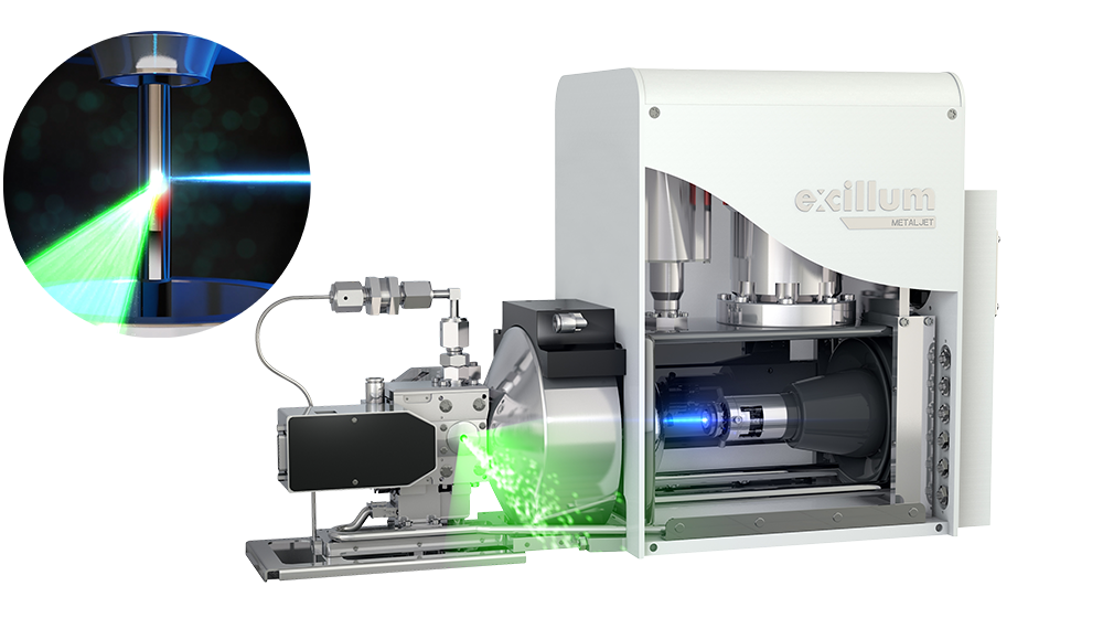
Figure 1: MetalJet D2+ – The world’s brightest home lab X-ray source for SC-XRD.
The MetalJet D2+, as illustrated in Figure 1, is currently the brightest home-lab X-ray source for SC-XRD. A very small primary focus of the source coupled with pre-figured synchrotron grade optics enable a high intensity beam delivery of only 50-micron diameter. As illustrated in Figure 2, a smaller and more intense beam means more photons on the small crystal while minimizing parasitic scattering from holder or air. This has tremendous effect on signal to noise ratio and greatly helps in the pursuit of measuring smaller crystals using SC-XRD. Furthermore, with the latest introduction of Dynamic Adaptation (DA) technology in the MetalJet D2+, a uniquely precise focal spot control is obtained, that will enable crystallographers to take full advantage of the new innovations and bring routine structure determination from micron sized crystals ever closer to reality.
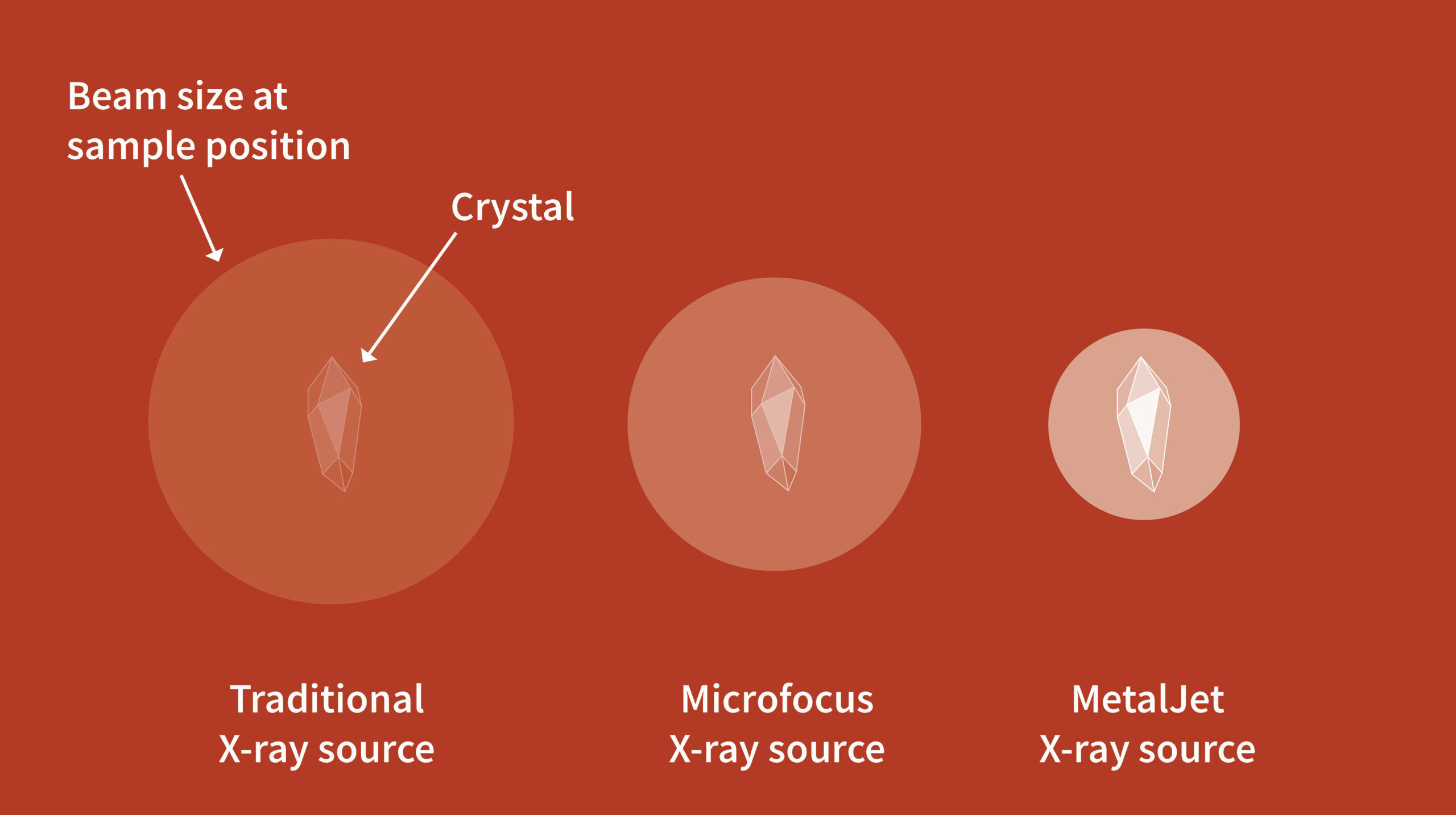
Figure 2: Schematic representation of beam size and intensity for different X-ray source technologies.
Combining the MetalJet with photon-counting detectors means that data quality comparable with that collected at synchrotrons is achievable, and also that crystals of similar size can be measured on the MetalJet D2+ as many modern beamlines [2-5]. The primary difference is the time required to collect data being measured in minutes rather than seconds.
SC-XRD is currently experiencing a period of great innovations, triggered by the collection of data at room temperature at X-ray free electrons sources (XFELs). The need to find new ways to deliver crystals into the beam and collect data on XFELS has stimulated development of methods in serial crystallography (SX) at synchrotrons [6] which can also be applied to home-lab instruments with ultra-bright sources such as the MetalJet. New tools and techniques for mounting barely visible crystals into the X-ray beam are also under development [7].
Nano-crystallography with 3D electron diffraction
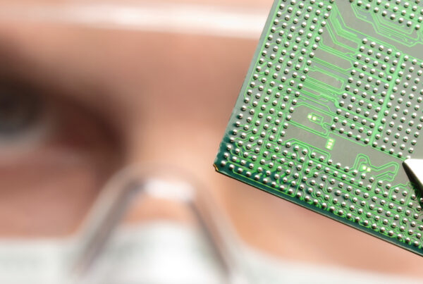
Electron diffraction also known as ED, 3D ED or microED emerges as a powerful supplementary technique, primarily attributed to the strong interaction between electrons and matter which facilitates collecting diffraction data with high signal to noise ratio from crystals with nano- or submicron-dimensions [8]. When the crystal is not thin enough, however, the multiple scattering events called dynamical effects have significant impact on the intensities of Bragg reflections. The genuine advantage of 3D ED is mainly where crystals larger than 1 micron are simply not possible to grow. Crystals with several micron thickness are often considered impracticable for 3D ED methods [9], thus techniques such as cryo-FIB or physical fragmentation are sometimes adopted to get small enough crystal size for 3D ED.
Besides the advantage of small crystals, it’s easier for 3D ED than SC-XRD to locate atoms like lithium and possibly hydrogen since electrons are more sensitive to light atoms when compared with X-rays. The positional accuracies are closer to those from neutron diffraction, but it’s worth noting that dynamical refinement is required for such high accuracies locating light atoms. Dynamical refinement also has strong sensitivity to the absolute configuration of chiral structures, which are extremely important in pharmaceutical applications. 3D ED also has advantages in making use of its combined imaging and diffraction capabilities implemented as a method called crystal mapping. This technique screens particles by STEM with subsequent continuous rotation diffraction and is suitable to identify and characterize the presence of polymorphs, phases and impurities in mixtures of crystalline and amorphous compounds [9].

Figure 3: Excillum electron source with horizontal electron beam and a highly simplified design compared to standard TEM system.
3D ED has been rapidly developed in the past decade. Most of the development has previously been done on traditional transmission electron microscopes (TEMs). These microscopes are high end instrumentation with significant infrastructure demands and a complex electron optics design. This meant that 3D ED was very time demanding and that in principle very highly trained experts were needed both for 3D ED measurements and the subsequent analysis [10]. In the recent years however the introduction of the ELDICO ED-1 as a dedicated electron diffractometer with an electron beam system (electron source and optics) from Excillum (see Figure 3) has overcome many of these obstacles and demonstrates a remarkable simplification in the measurement workflow. The Excillum electron beam system was specifically developed in partnership with ELDICO for 3D ED applications, allowing an easy switching between a focused beam for low dose STEM (scanning transmission electron microscopy) imaging and a parallel beam for diffraction. In addition, this development came with a great simplification of the electron optics with a horizontal geometry enabling both easy and robust operation as well as the possibility for a goniometer with a vertical rotation axis. The vertical rotation axis allows for higher precision (lower sphere of confusion) which is crucial to keep the extremely small crystals in the electron beam, which typically has a diameter below 1 micron. With the introduction of dedicated electron diffraction equipment the technology of 3D ED and structure determination from sub-micron crystals are therefore quickly opening up to a wider community.
Conclusion
Developments in both X-ray and electron diffraction nowadays provide the crystallographer with home lab tools to address crystals of all sizes. In addition, both electrons and X-rays have their respective advantages and both techniques are truly complementary. Excillum is proud to assist the crystallographic community with both the world’s only dedicated electron source solely made for electron diffraction as well as the brightest X-ray source in the world.
Acknowledgements
The authors would like to thank Dr. Vernon Smith from Bruker AXS, and Dr. Christian Jandl and Dr. Petra Simoncic from Eldico Scientific for valuable input to this article.
References
[1] F. A. Almeida Paz, Structural Determination of a Two Micron-sized MOF Crystal, Bruker Application note SC-XRD 502.
[2] P. Krafcikova et al., Nature Communications, (2020) 11:3717.
[3] T. M. Moon et al., The structures of penicillin binding protein 4 (PBP4) and PBP5 from Enterococci provide structural insights into b-lactam resistance, J. Biol. Chem. published online October 24, 2018.
[4] J. P. Durrant et al., Dominance of Cyclobutadienyl Over Cyclopentadienyl in the Crystal Field Splitting in Dysprosium Single-Molecule Magnets, Angew. Chem. Int. Ed. 2022, 61.
[5] GPCR Crystallography Moves In-House: Structure of the Human Orexin-1 StaR® to 2.77 Å, Bruker Application note SC-XRD 514.
[6] P. Mehrabi et al., Serial femtosecond and serial synchrotron crystallography can yield data of equivalent quality: A systematic comparison, Sci. Adv. 2021; 7.
[7] G. Illava et al., Integrated sample-handling and mounting system for fixed-target serial synchrotron crystallography, Acta Cryst. (2021). D77, 628–644.
[8] T. Gruene, E. Mugnaioli, 3D Electron Diffraction for Chemical Analysis: Instrumentation Developments and Innovative Applications, Chem. Rev. 2021, 121, 11823−11834.
[9] Merkelbach et al., Crystal mapping by continuous rotation electron diffraction, Imaging & Microscopy, 2023, 3, 31-33.
[10] P. Simoncic et al., Electron crystallography and dedicated electron-diffraction instrumentation, Acta Cryst. (2023). E79, 410–422.
Authors: Dr. Shichao Hu and Dr. Julius Hållstedt, Excillum AB
Contact us
If you would like to know more, please don’t hesitate to contact us.