Sharper scans, faster ramp-up
How a leap forward in X-ray resolution can drive development and boost yield in advanced packaging
High-density interconnects. Micron-scale solder bumps. Sub-micron defects. As semiconductor architecture grows more complex with 3D heterogenous integration and ever decreasing dimensions, critical reliability issues arise with smaller defects. To achieve faster prototypes and improve ramp-up yield, the next generation of inspection tools need a major increase in 3D imaging resolution down to sub-micron level.
New strategies are emerging to meet demands for ever smaller, more powerful, and more efficient semiconductor packaging. Yet, as 2.5D and 3D stacked chips move through their design, prototype and manufacturing phases, the root causes of failures are becoming more difficult – and more costly – to detect using destructive test methods alone.
150 nm resolution is here
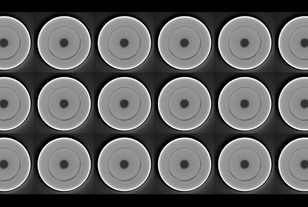
Fortunately, new advances in X-ray imaging make it possible to capture high-resolution 3D images of bump bonds, vias and other critical features with sub-micron precision. Using a NanoTube N3 X-ray source with the world’s smallest X-ray spot size, down to 150 nm resolution can be achieved using simple geometric magnification. This is illustrated by the reference patterns of a JIMA resolution chart and Siemens star, resulting in highly detailed metrology that is simply sharper and more multidimensional than any other inspection method to date.
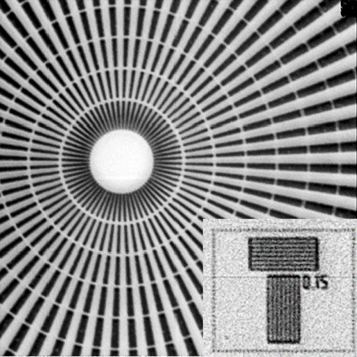
The best way to prove the resolution performance of an imaging system is to use resolution targets. Here are images of 150 nm lines and spaces on a JIMA resolution chart (insert) and a Siemens star test pattern, with innermost features of 150 nm as imaged by the NanoTube. This demonstrates the truly round spot of the NanoTube, achieving 150 nm resolution.
Crystal clear 2D and 3D imaging
To illustrate the possibility of high-resolution X-ray metrology we take a look at two different examples.
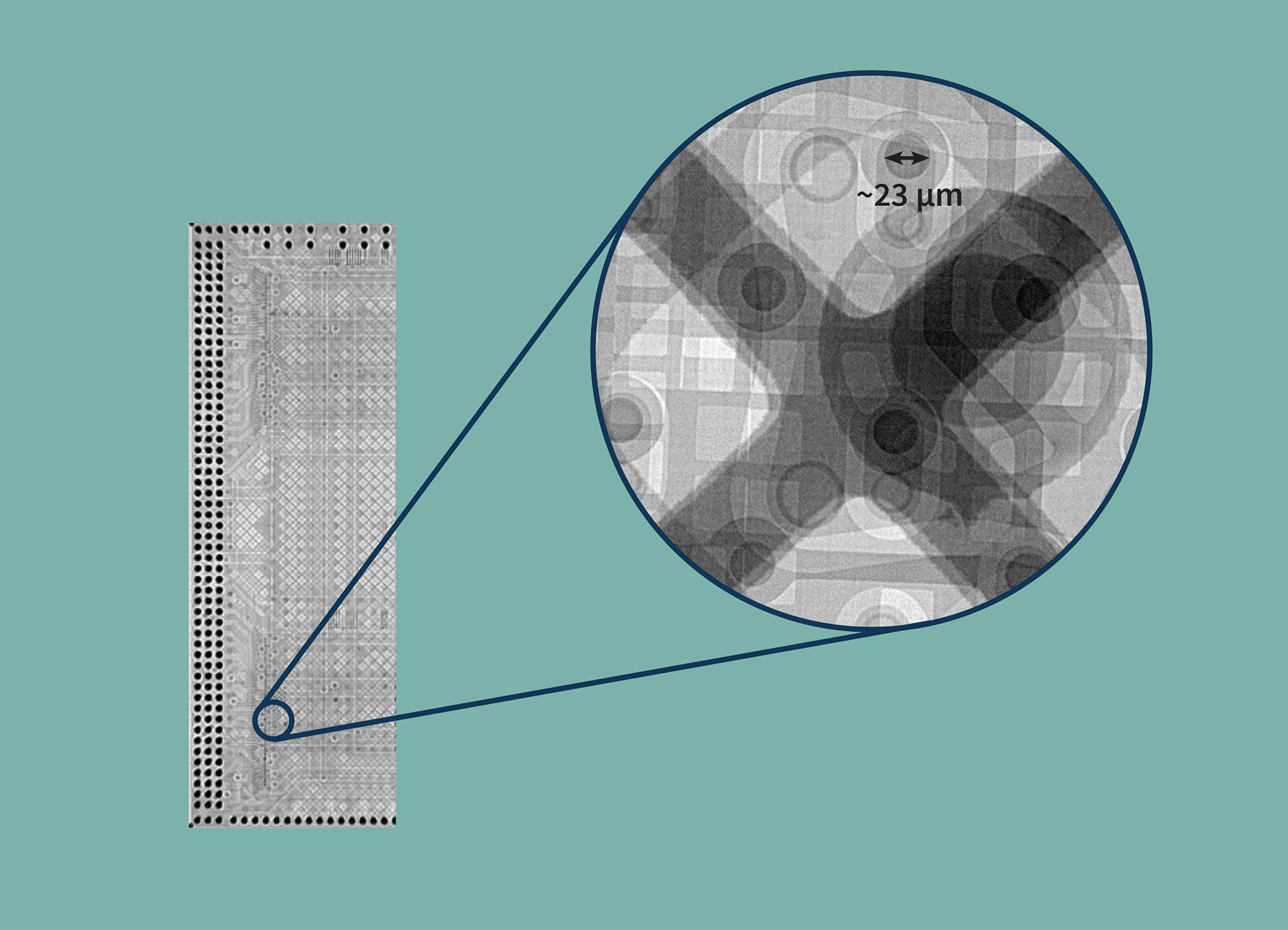
System on chip package
For the system on chip (SoC) package, an A15 chip, a quick 2D radiography was performed from top and side. Features of even the smallest components of ball grid arrays (BGA) or wire bond connections are clearly visible enabling early detection of quality and yield issues.
Side view
Top view
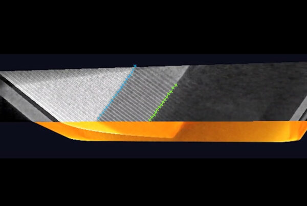
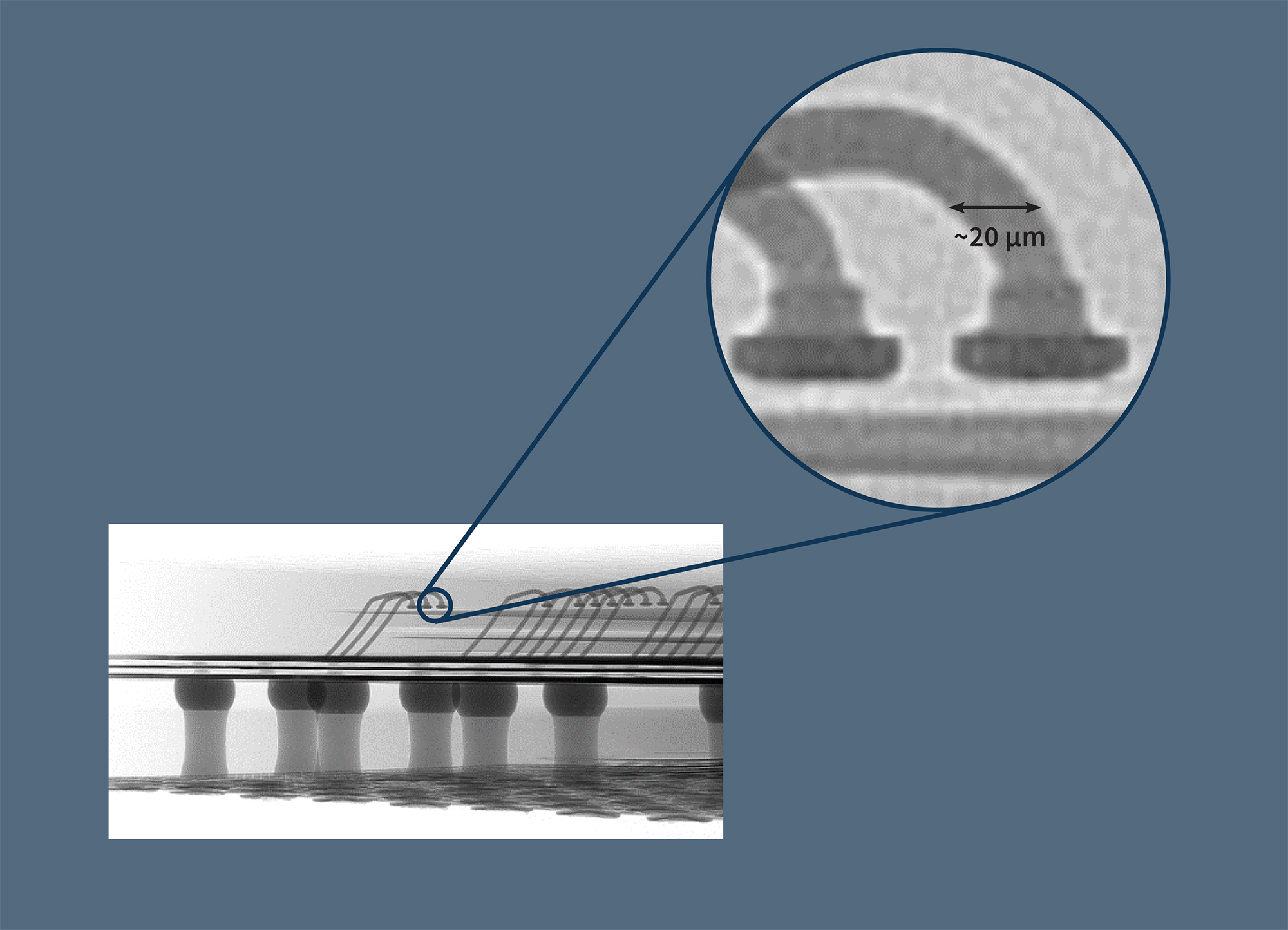
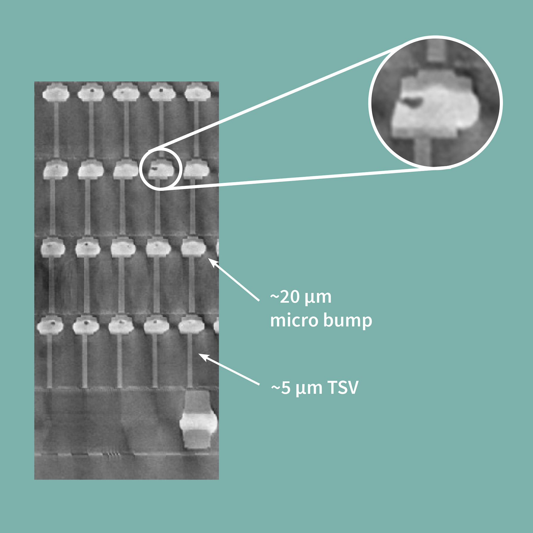
Commercial GPU with 8 layers of High Bandwidth Memory (HBM)
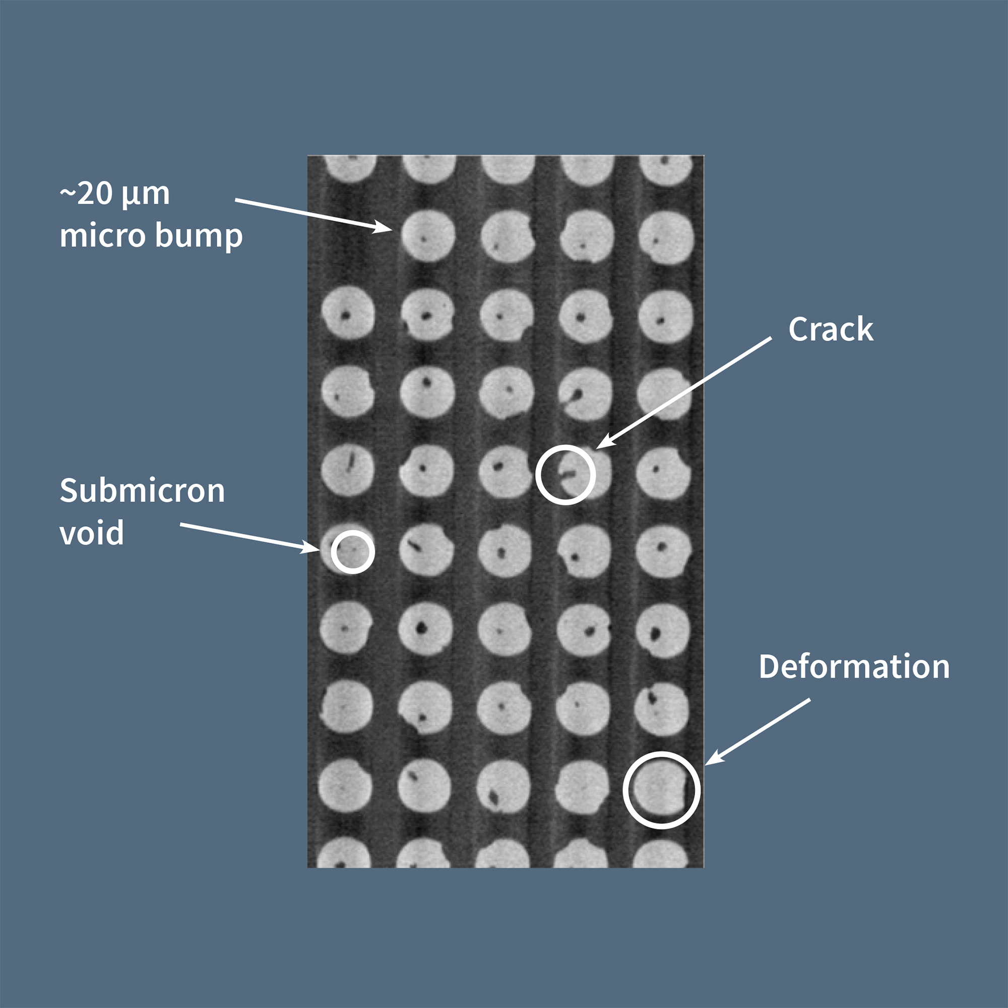
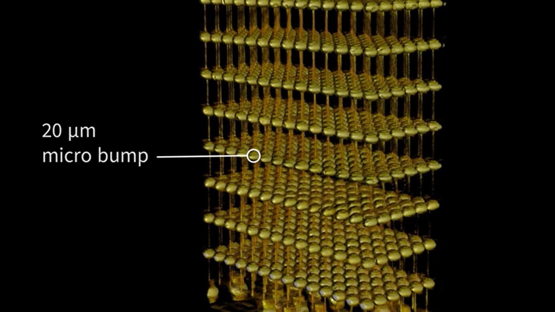
The HBM consists of a stack of memory modules connected via Through Silicon Vias (TSV) and thousands of micro bumps, where the performance and reliability of the unit relies on good electrical contact between each micro bump and TSV . In the competition for increased bandwidth and computing power, every new generation of interconnects for HBM continuously decreases in size and pitch. The development roadmap outlines the evolution of packages into fully 3D assemblies, including more memory, logic, and exotic integrated devices, resulting in increasingly dense and complex advanced packaging assemblies.
Extreme resolution X-ray imaging such as nano-CT or planar-CT/ laminography is therefore essential both for today’s and future technology to adequately analyze the full device with all layers and components in 3D, particularly when identifying sub-micron sized voids, cracks, misalignments, and other defects.
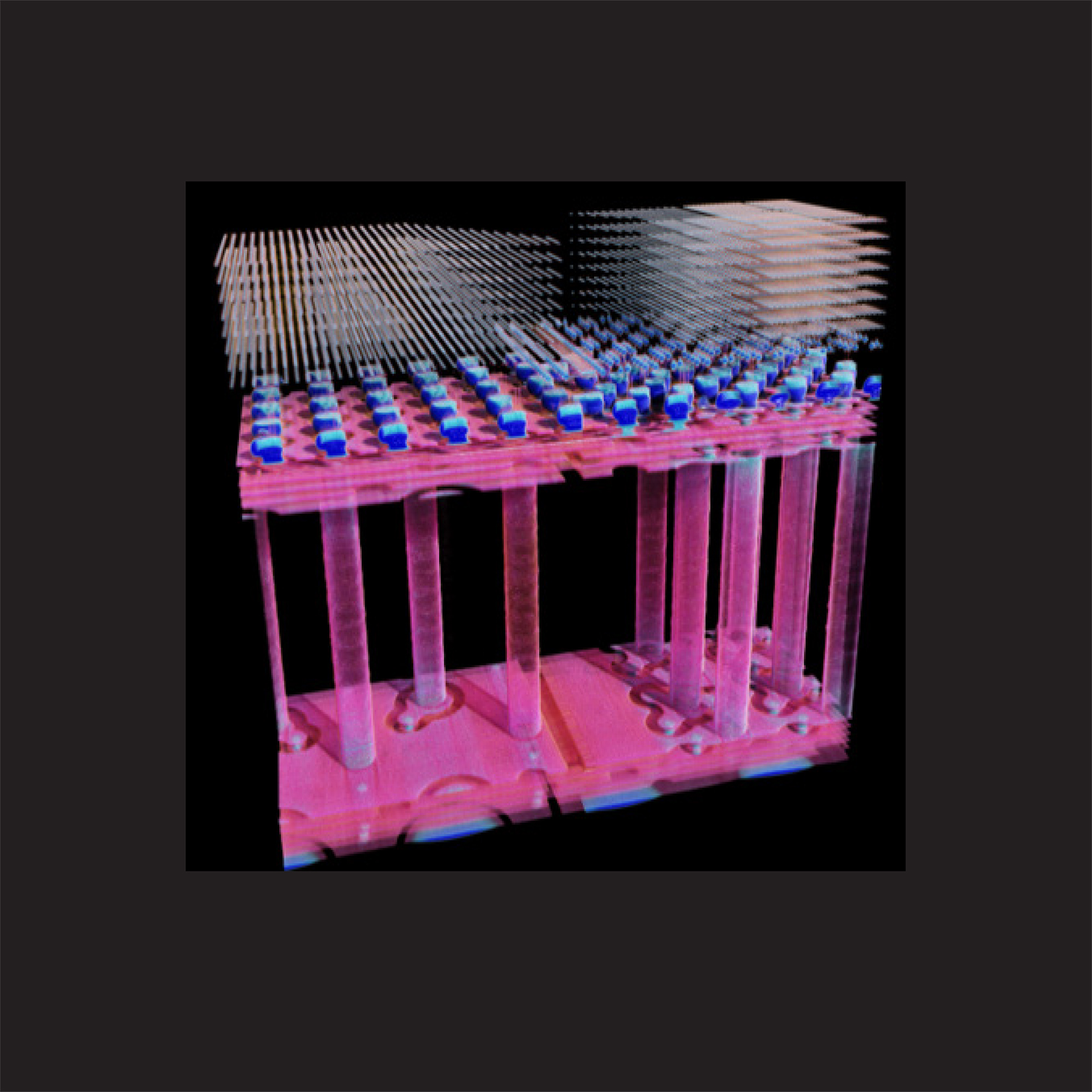
The following images acquired using the NanoTube N3, illustrate first the reconstructed 3D render from an overview scan and then a vertical and horizontal slice from a Region of Interest (ROI) scan of an HBM memory module. Features of TSVs and micro bumps are clearly visible and several voids and defects within a series of 20 µm micro bumps. The clarity in the image demonstrates the unparalleled performance of using the NanoTube N3 source for the investigation of advanced packaging assemblies.
Watch video of 3D X-ray with NanoTube N3 for advanced packaging.
Better resolution for improved failure analysis
The reconstructions made from the NanoTube N3 represent a significant improvement in resolution over any alternative nanofocus X-ray source. This enables the possibility to virtually reconstruct the full 3D volume of the advanced package which can then be sliced and examined from any angle and in any direction. In failure analysis labs, this translates to faster and more precise identification of defects and their root causes.
Taking MXI and AXI metrology to the next level
For yield and quality control/assurance (QA/QC) in manufacturing, both manual (MXI) and automatic (AXI) X-ray inspection are utilized, analyses rely on both resolution and measurement speed. The fast, easy and accurate switching of the X-ray spot size and acceleration voltage in combination with market-leading X-ray power enable optimized parameters to be set for each measurement. The result is faster and more reliable data of higher precision that can be used to detect defective assemblies early to minimize production cost, avoid expensive recalls, and warranty claims. Furthermore, the wealth and details of the data can continuously monitor trends and avoid/minimize critical defects before they appear which can be fed back into the R&D process to improve yield in ramp-up to full-scale manufacturing.
Why X-ray spot size matters
In the world of X-ray inspection, the source spot size, stability, and brightness are critical in enabling the highest possible image resolution in the shortest amount of time. The NanoTube N3, which combines high X-ray flux with exceptional spot stability and quality, is controlled by an automatic e-beam focusing and astigmatism correction system to consistently maintain the smallest possible, truly round spot during day-to-day operation.
The result is a dramatic increase in imaging resolution compared to other X-ray sources, with an unprecedented true resolution of 150 nm lines and spaces. Whereas previous generations of X-ray metrology systems were once seen as either too slow or too low-resolution for the demands of failure analysis and quality control in advanced packaging, these barriers are now long gone.

Illustration of the spot size effect on the resolution, commonly known as the penumbra effect. The larger the spot size the blurrier and more undefined image.
Whether the aim is to understand failure mechanisms, improve design or increase yield in next-generation 3D heterogenous integration, a new era of nanoscale technologies demands a leap forward in nano-CT and laminography resolution. Thanks to NanoTube N3, the path forward for advanced packaging inspection is clearer than ever before.
Author: Dr. Julius Hållstedt, Excillum AB