In 2025, it is now clear to those who manufacture semiconductor devices that the path to enhanced performance, lower power consumption and lower cost per function lies in chiplet integration using advanced packaging technologies. However, as package feature sizes shrink and interconnect densities grow, ensuring manufacturing quality and reliability has become more challenging than ever. Efficient fault isolation, failure analysis, yield improvement and quality control all rely heavily on advanced characterization and metrology tools—where X-ray imaging plays a crucial role. From early-stage process development to high-volume production (lab to fab), X-ray inspection provides the 3D visualization and capability for non-destructive insights needed to evaluate hidden structures, identify defects, and optimize manufacturing processes.
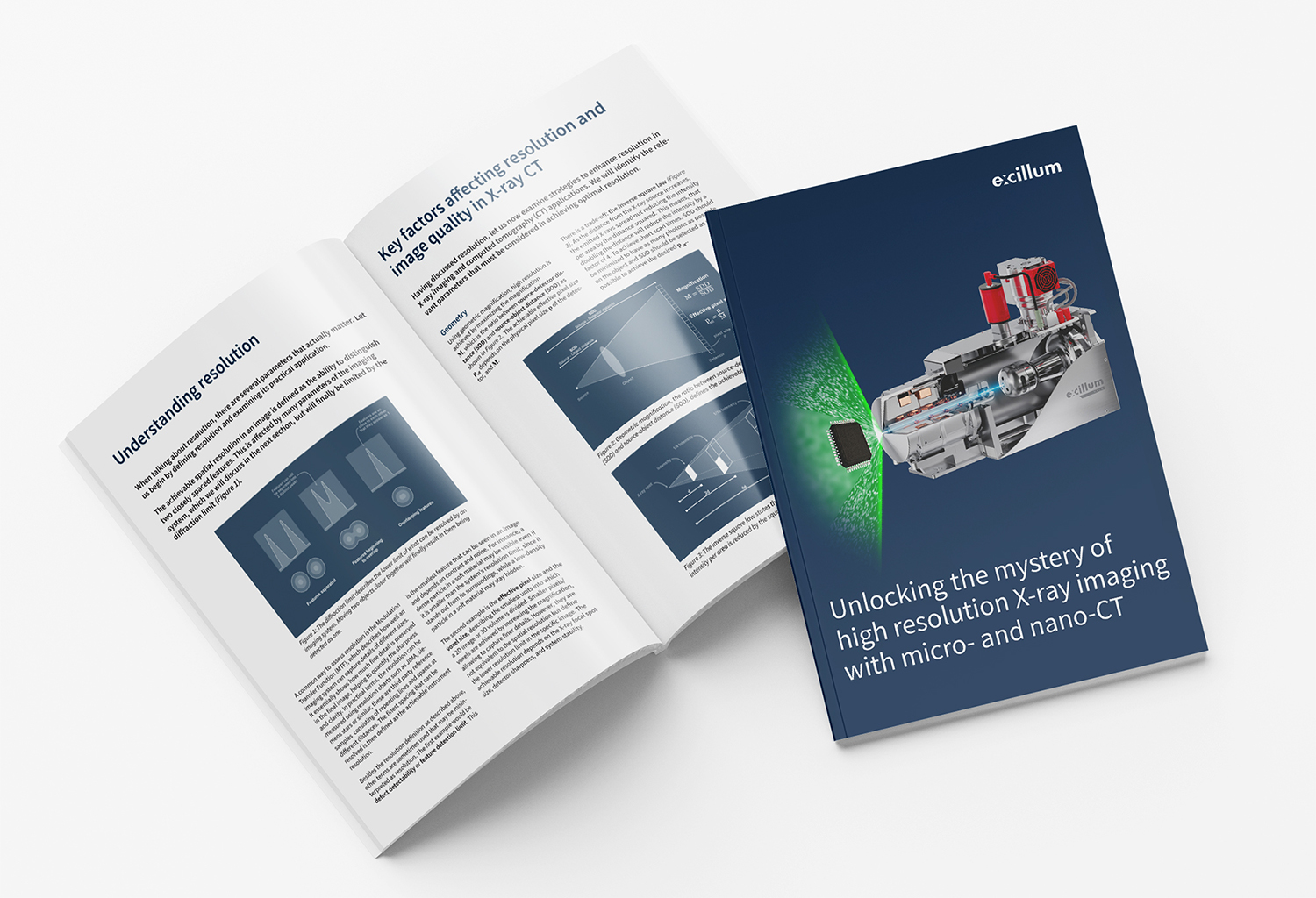
This article provides the background on the key design considerations necessary to maximize the potential of 3D X-ray methods for electronics R&D and manufacturing. It outlines the fundamental principles of X-ray imaging, explores critical factors influencing measurement performance, and discusses best practices for optimizing setups based on geometric magnification. By understanding these factors, engineers and researchers can unlock the full capabilities of X-ray technology.


