Semiconductors & electronics
Sharper scans, faster ramp-up
Some say that Moore’s law, which says that the number of transistors in a dense integrated circuit doubles about every two years, has reached its limit. That the size and complexity of today’s surface mount technologies (SMT) makes continued exponential performance gains unlikely, but the technology drivers continue along this path, with transistors becoming ever smaller.
Excillum X-ray sources allow manufacturers to push beyond the limits of even today’s most state-of-the art X-ray techniques. Combined with other leading-edge components, Excillum X-ray sources have the power, imaging speed and resolution to produce the superior systems needed to inspect future generations of smaller, faster and more powerful electronic assemblies. The result is an entirely new standard in X-ray inspection for complex SMT, semiconductor and advanced packaging.
Interested in a demonstration?
Are you a manufacturer and want to know how to push beyond the limits of even today’s most state-of-the art X-ray techniques? Book a demo with us!
Book a demo
Application examples
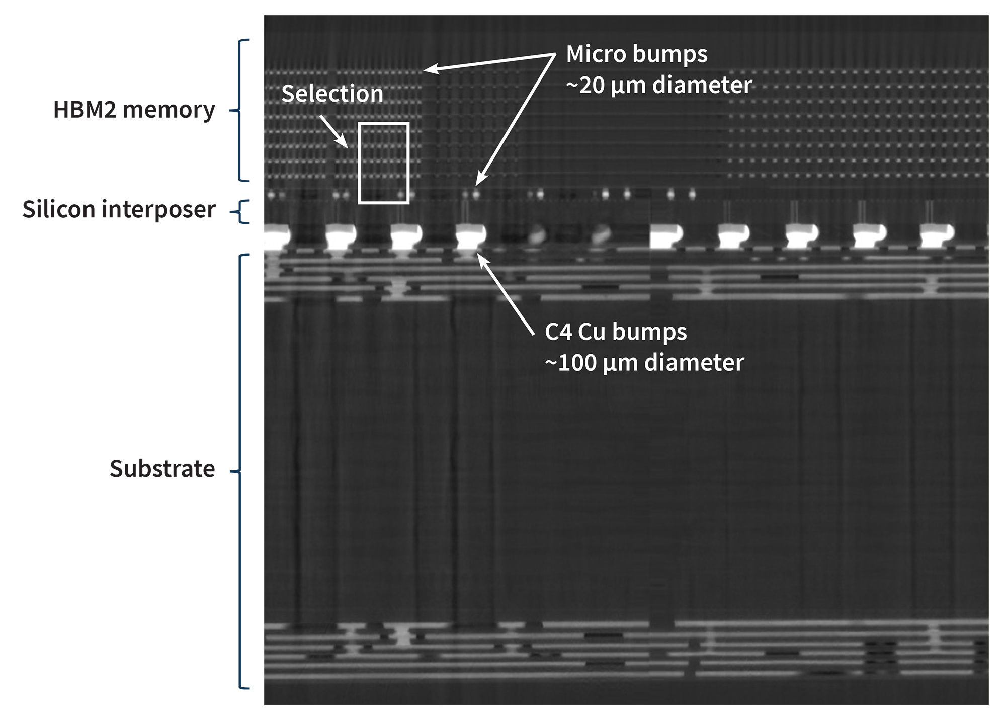
Extreme resolution nano-CT X-ray investigation of 3D memory (HBM2)
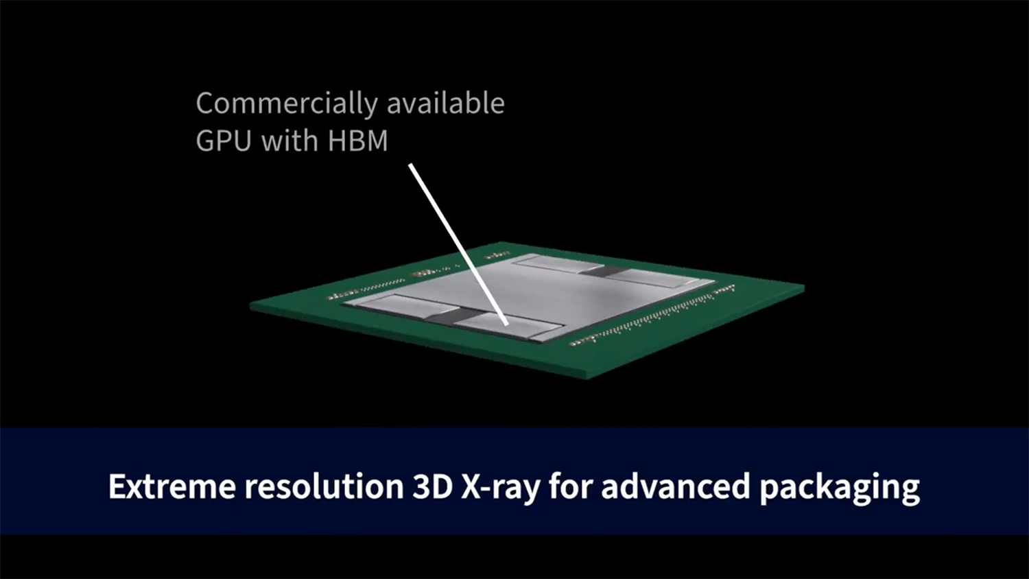
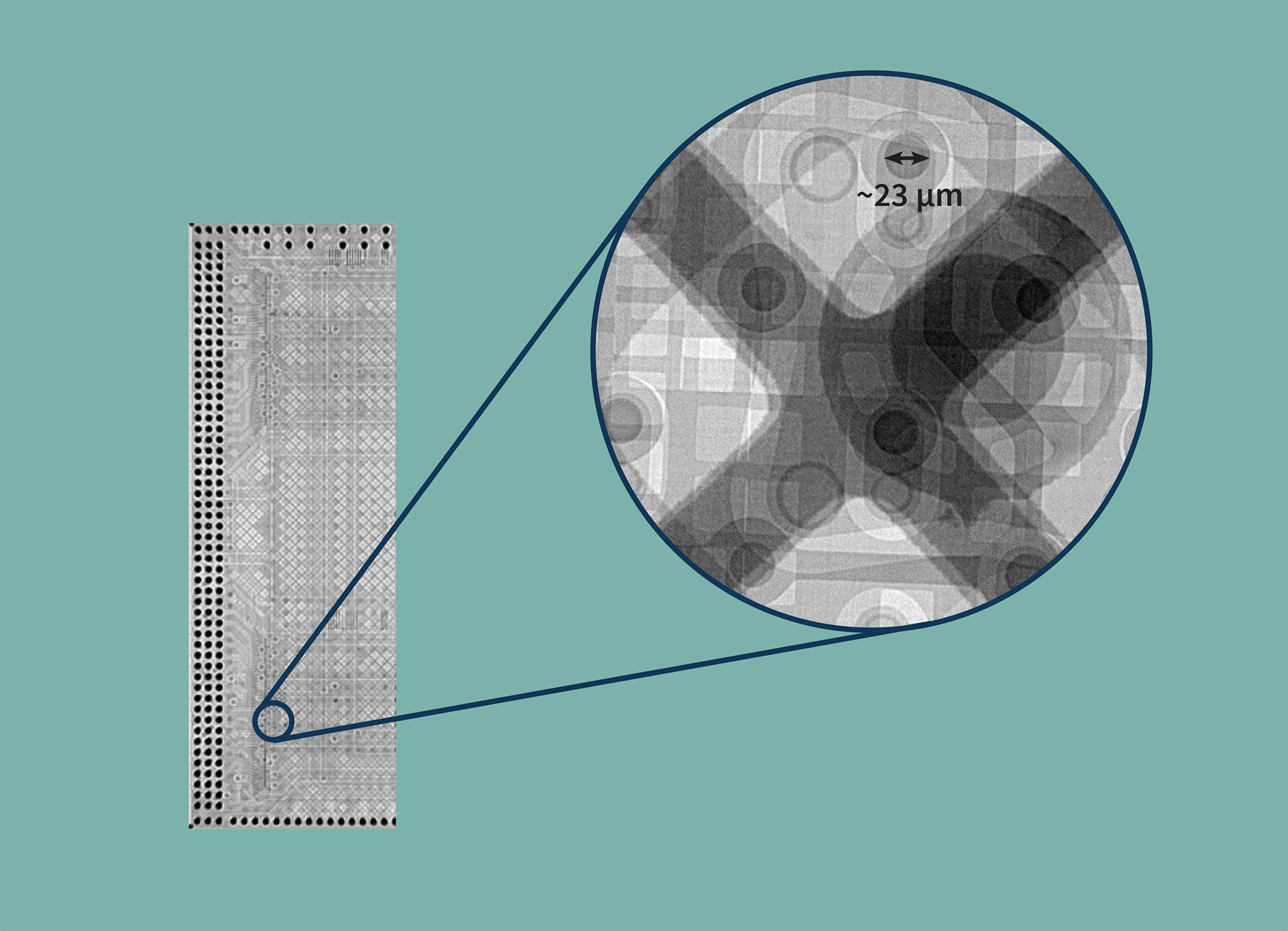
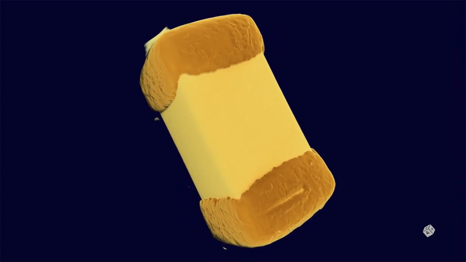
High Bandwidth Memory (HBM) micro bumps are used in advanced packaging in order to accommodate extremely fast data transfer between a GPU and HBM. The HBMs are stacked on top of each other close to the GPU and connected with Through Silicon Vias (TSV) and small (~20 µm) micro bumps. The process is expensive and each package has high value. It is therefore of high interest to be able to measure and detect e.g. alignment and shift of TSVs or shape and defects (voids, cracks, non-wetting, bulge missing bumps etc) in the micro bumps. As an illustrative example a commercial GPU with HBM was analysed using the Excillum NanoTube N3 X-ray source in a nano-CT setup.
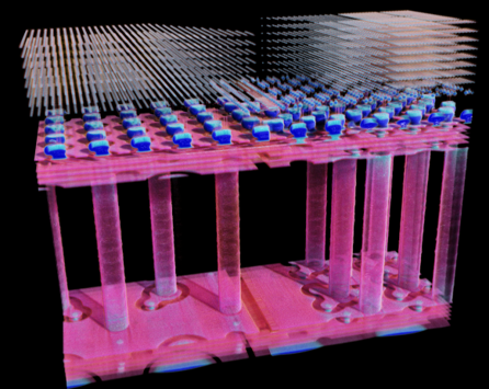
3D render of reconstructed volume.
Slice through volume showing all layers.
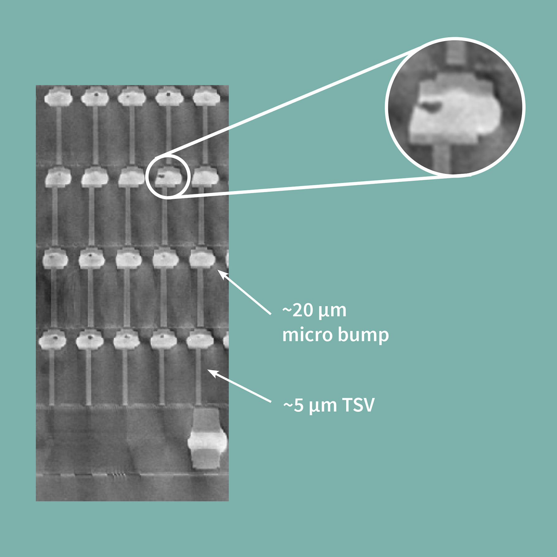
2D vertical cut of HBMs with TSVs and an extreme zoom-in on one of the micro bumps.
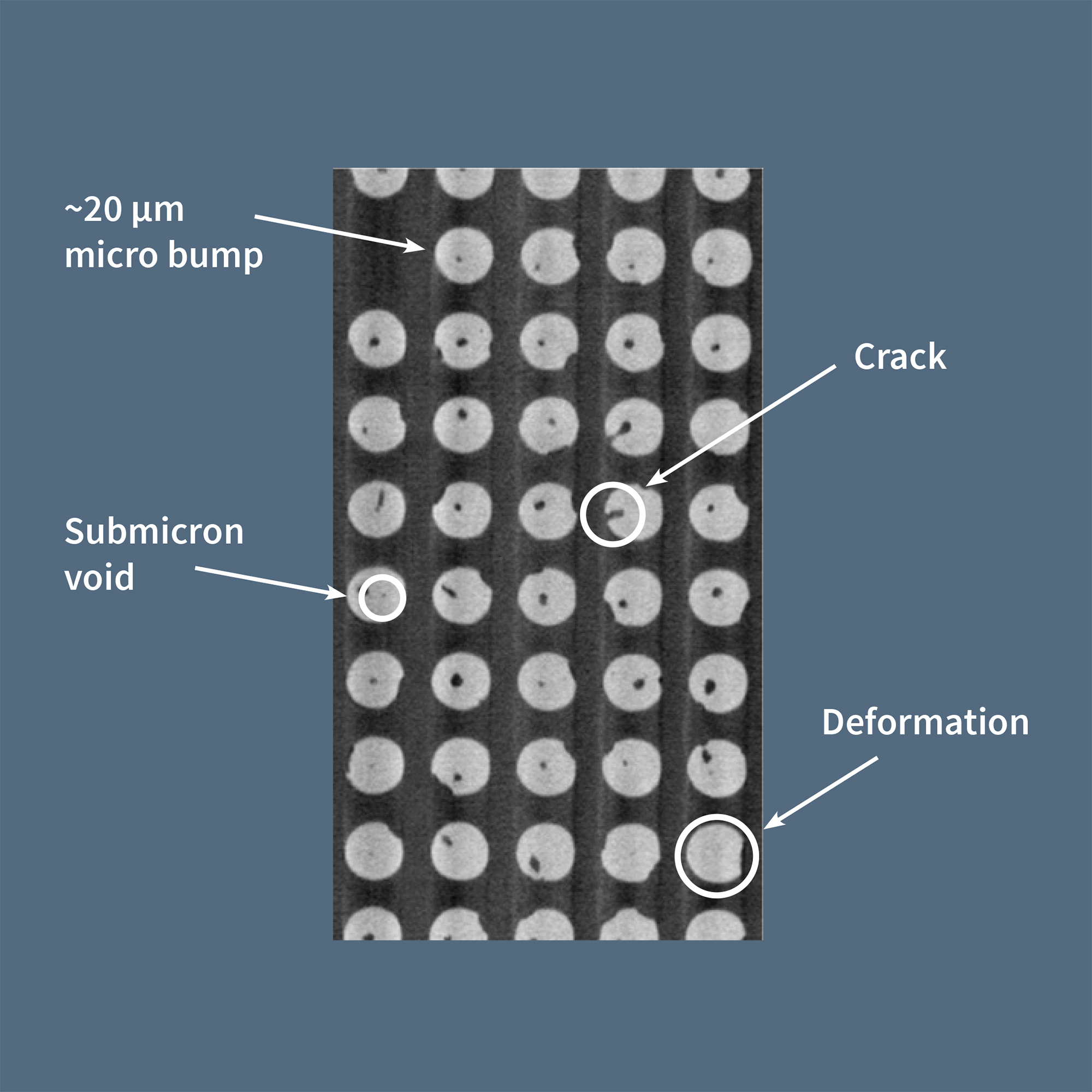
2D horizontal cut of micro bumps illustrating cracks and voids of different sizes.
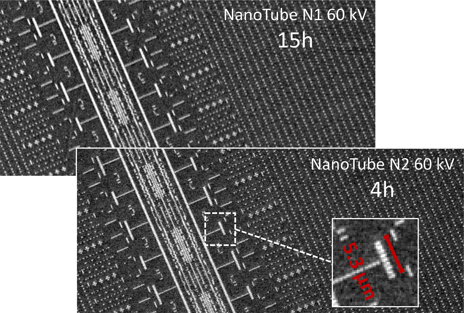
NanoCT investigation of SD card
With its small spot size, the NanoTube is ideal to study the ever-shrinking structures of electronics. This example, done with predecessors of our current NanoTube N3 series, shows a tomographic slice from a nano-CT of an SD-card, performed with the NanoTube N1 60 kV (top image) and the NanoTube N2 60 kV (bottom image) – achieving a voxel sampling of 200nm.
The comparative nano-CT measurement was done by keeping a similar level of photon counts. The NanoTube N2 60 kV achieves an increase in flux by more than 3 times and, thus, the measurement time was reduced from 15 hours to 4 hours. At the same time, the signal-to-noise ratio gave even higher image quality, due to the reduced motion within the CT measurement.
A 3D rendering of the above mentioned SD card, showing the full reconstruction of the internal features and structures. Voxel sampling 200 nm.
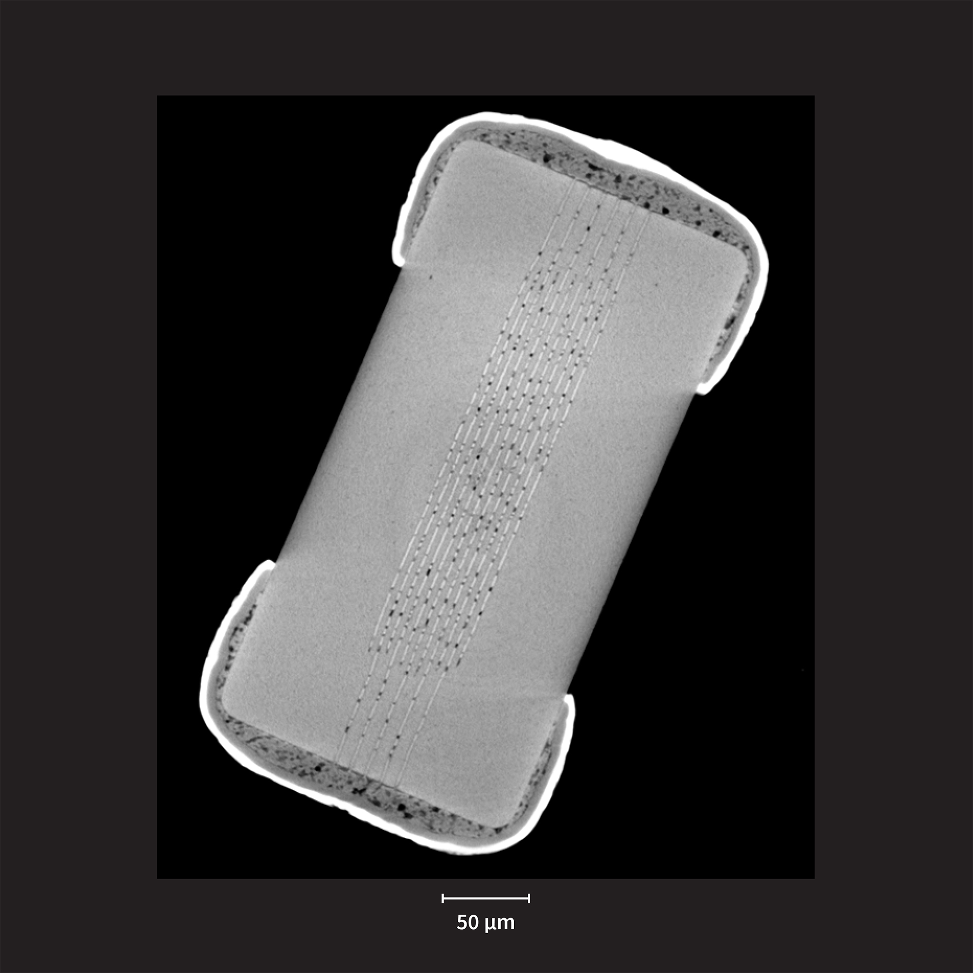
High resolution 2D electronics inspection of A15 system on a chip (SoC)
2D X-ray inspection of cell phone A15 SoC. In this study, a commercial 2D inspection system was used where the normal standard X-ray source was replaced by an Excillum NanoTube N3 X-ray source. The small and well-defined spot size makes it possible to create crystal clear images also of very small features. In addition, the fast and accurate switching between spot sizes enables the possibility to look at both large field of view as well as detailed zoom-ins.
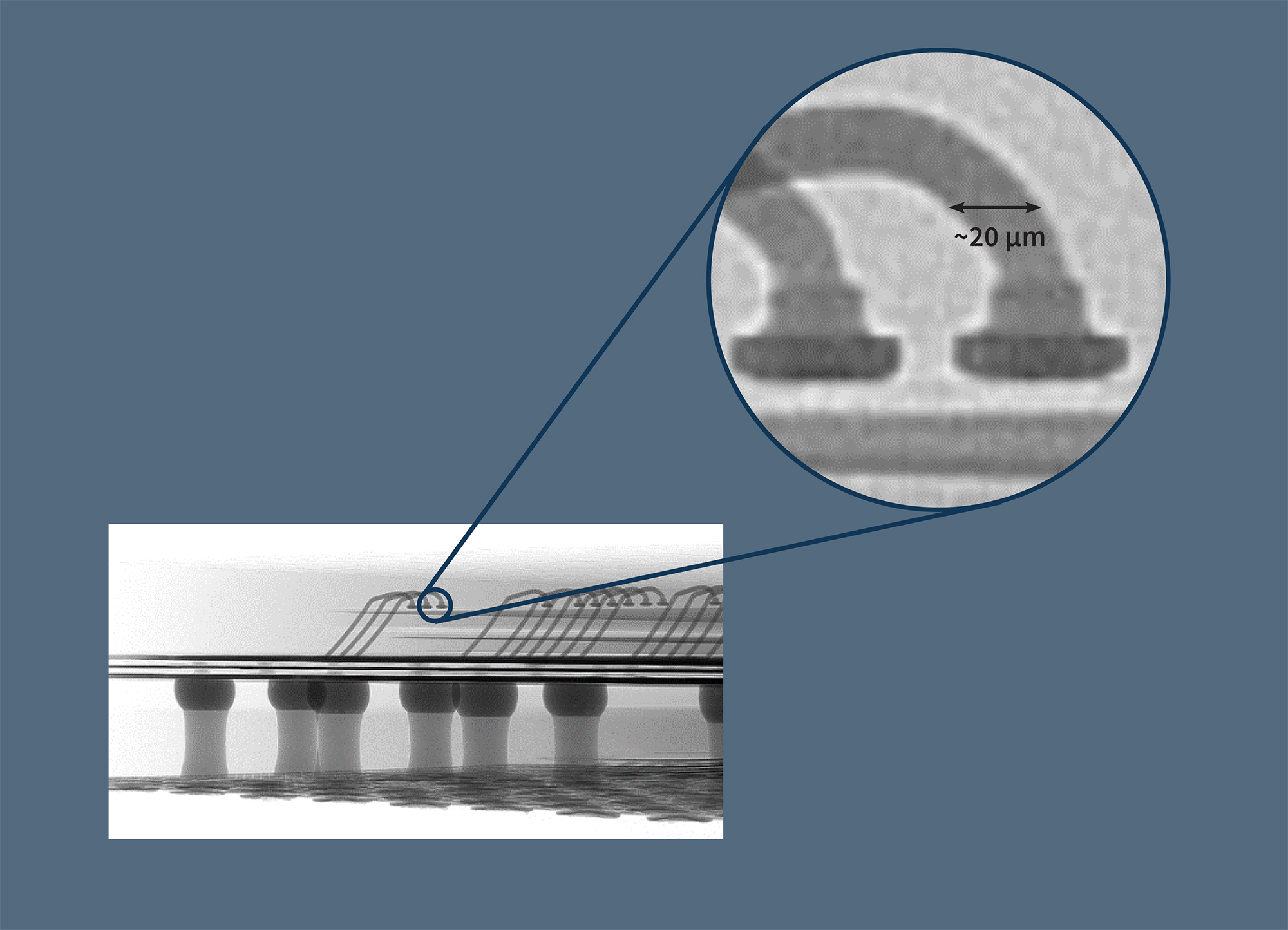
Side view of chip corner with zoom-in of 20 µm bond wire.
High resolution X-ray microscopy of Cu interconnects through X-ray optics
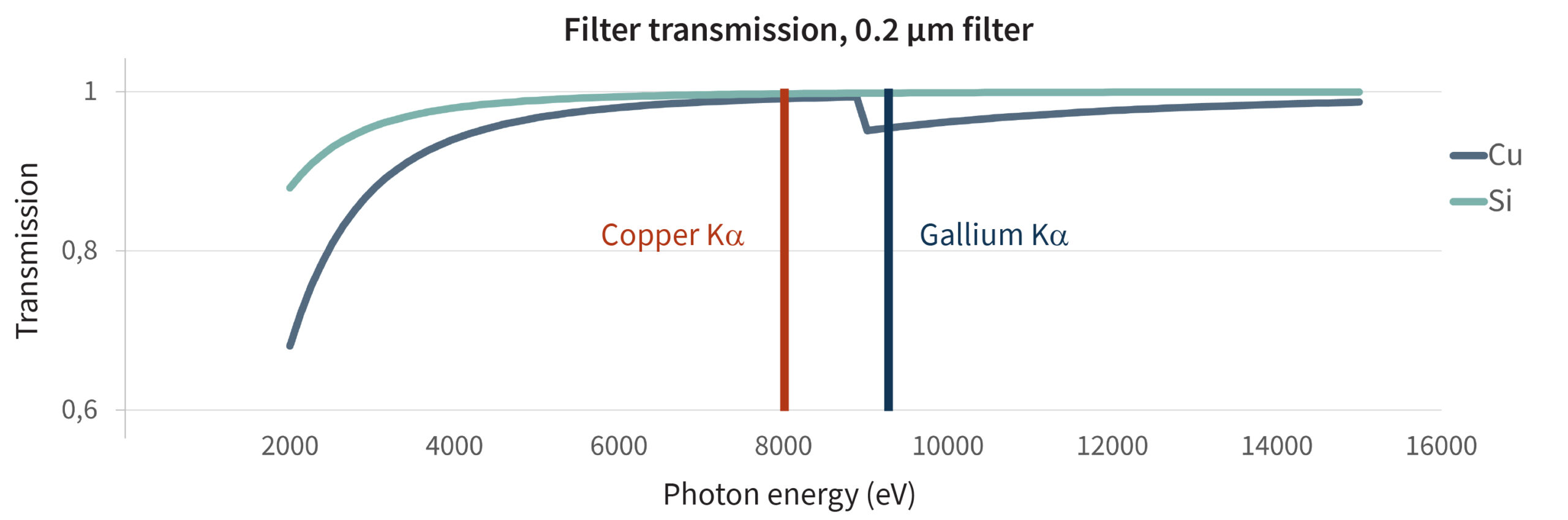
By applying X-ray optics it is possible to reach the best resolution. The setup involves condenser optic to increase the X-ray intensity on the sample then a zone plate or a laue lens projects the sample image on the detector. The X-ray optic is designed for a specific wavelength and using Gallium kalfa at energy of 9 keV which sits right above the absorption edge of Copper improves contrast on the smallest Cu features and enables resolution below 50 nm.
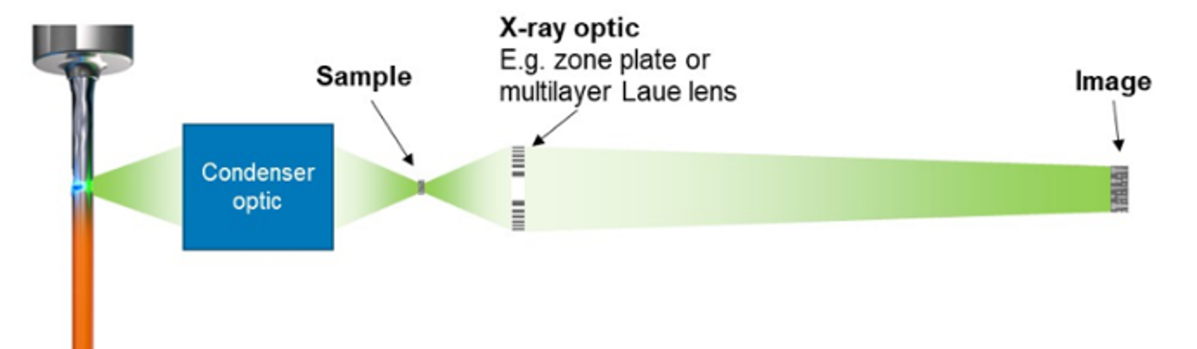
Schematic view of XRM setup.
Ga gives excellent Si/Cu contrast
MetalJet D2+ installed in Zeiss Xradia Ultra.
Image courtesy of Carsten Gundlach of Imaging at DTU, Denmark.
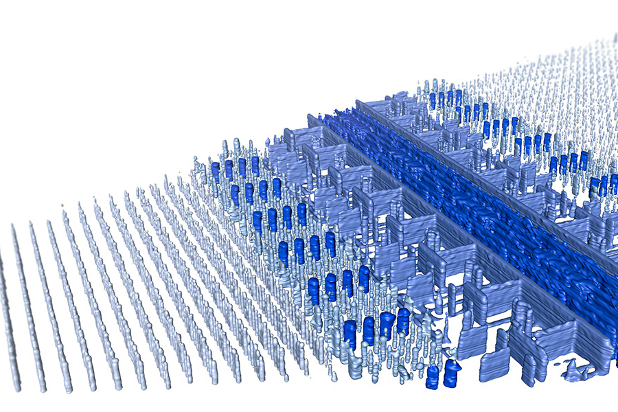
X-ray tomography of a 90 nm Cu process
(18x7 stitched overlapping tomographies)
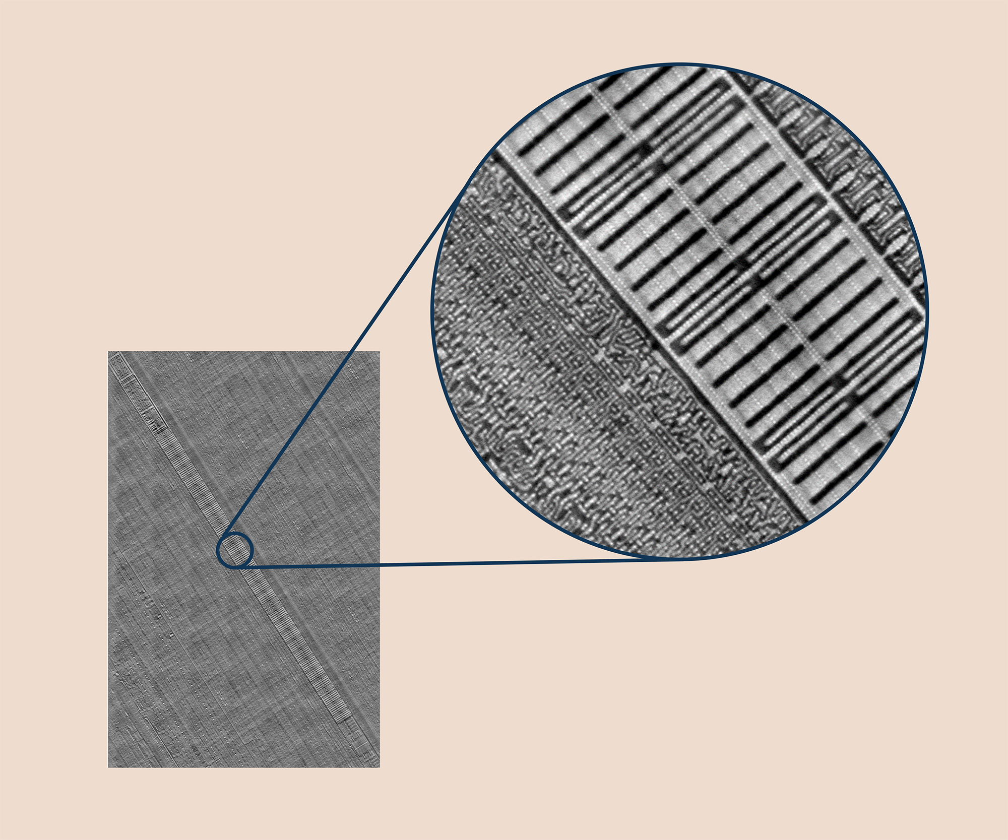
X-ray micrograph of one of the reconstructed layers. Zoom in provides detailed information of the Cu interconnects. Note that X-ray tomograhy provides 3D information on all layers. This illustrates a 2D representation of one layer.
Image kindly provided by Michael Sutherland – DMEA
Multi-layer ceramic capacitors (MLCC)
Multi-layer ceramic capacitors (MLCC) are vital components in electronic devices constructed of two or more alternating layers of ceramic and metal layers. As illustrated in the video and pictures below, by utilizing the NanoTube N3 in a nano-CT (3D X-ray) setup it is possible to get full internal 3D information of the MLCC at unprecedented resolution, revealing intricate internal structures and defects with unmatched clarity. The MLCC in this example is a 01005 component approximately 400 x 200 µm in size. This enables failure analysis or quality assurance at a previously unattainable level.
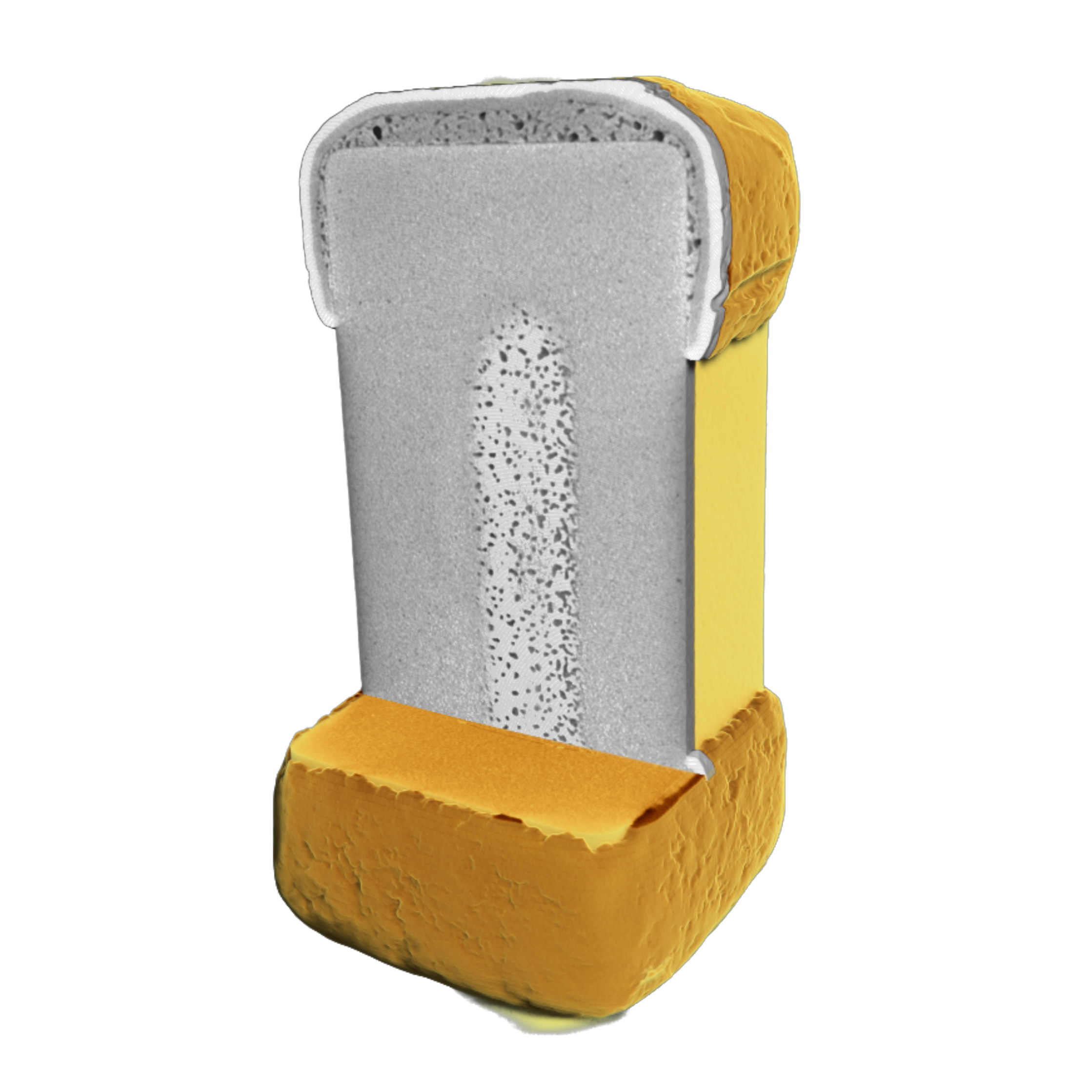
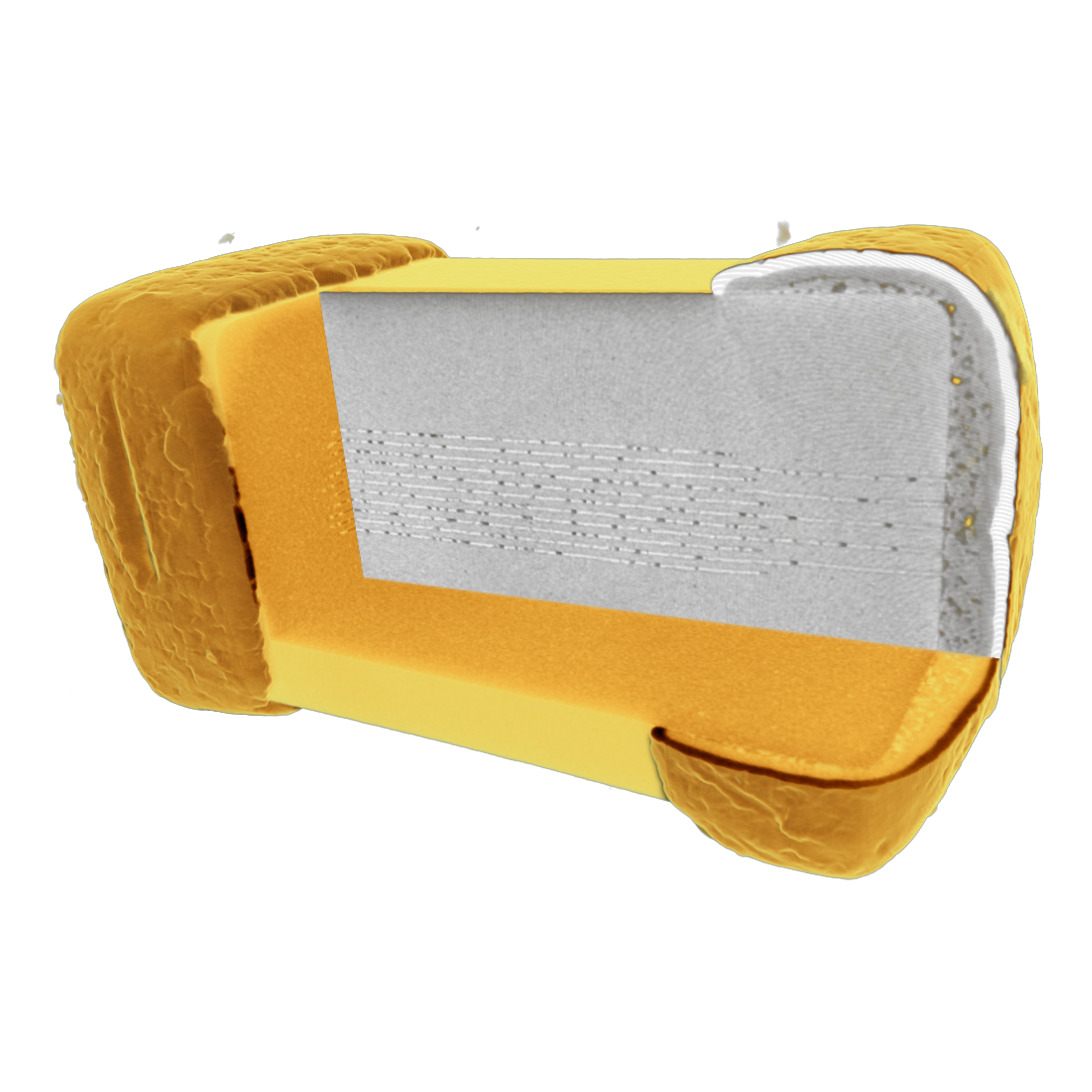
3D render with virtual cuts in two different directions.
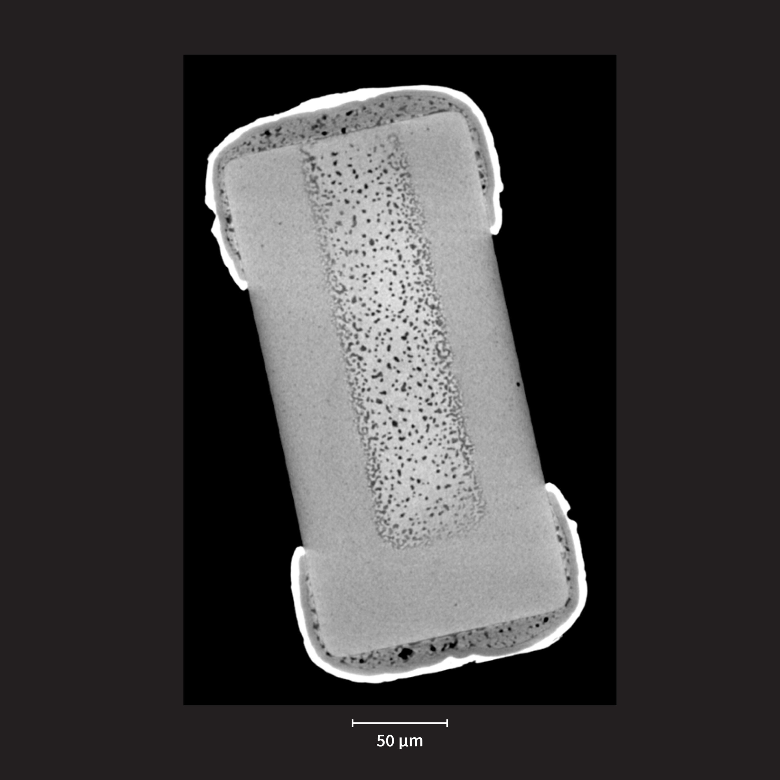
Detailed virtual slice through one of the 1.5 µm thick metal layers illustrating the defect level.
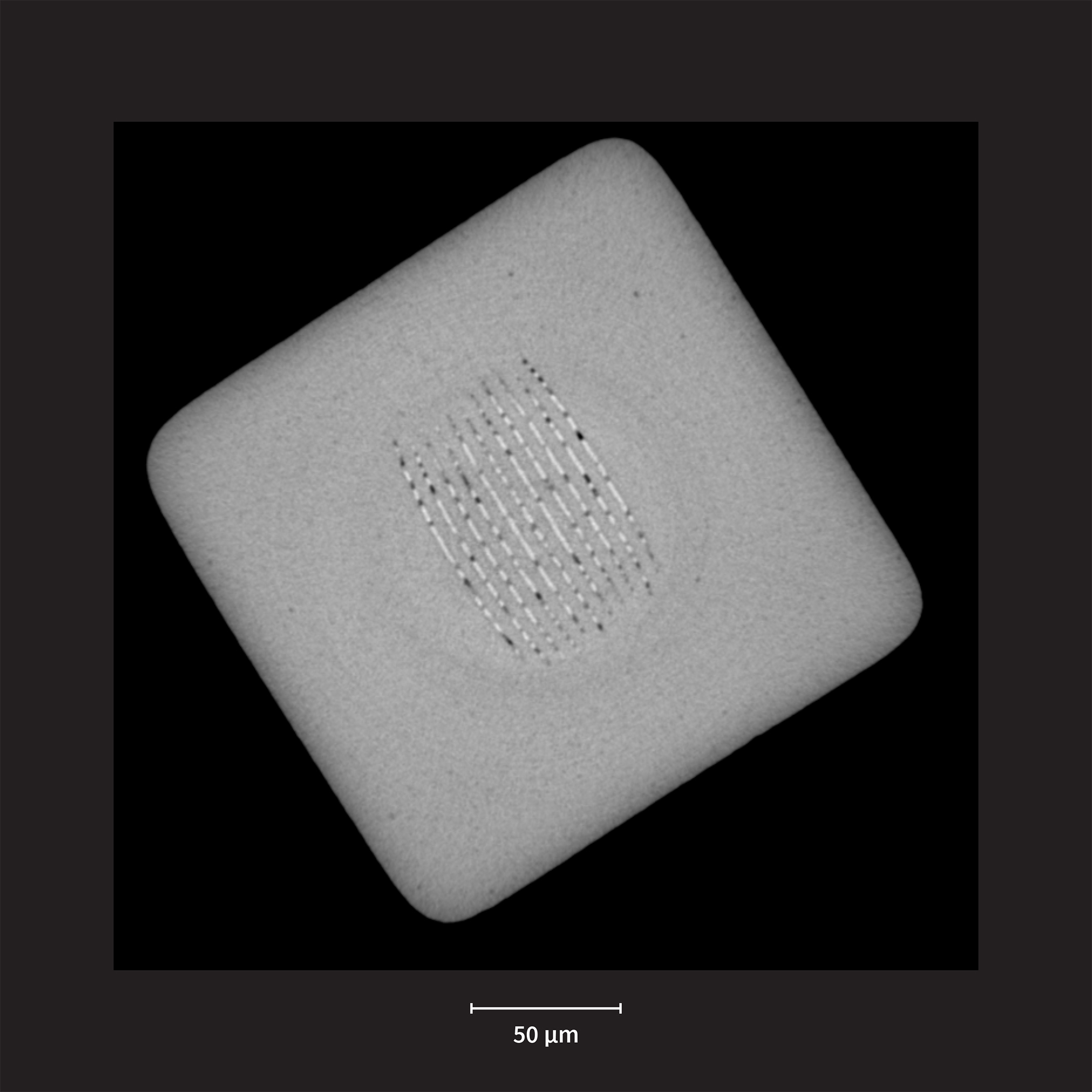
Virtual slice through the MLCC metal layers. The individual metal layer is approximately 1.5 µm thick.
Hybrid bonds
A commercially available AMD Ryzen 7 5800X3D was investigated. This device assembly utilizes hybrid bonds to attach SRAM cache memory vertically atop the processing core. The hybrid bonds are 1.5 µm in diameter at 9 µm pitch and approximately 15 µm length. Due to the small size and tight pitch hybrid bonds are considered challenging for X-ray investigation.
In this investigation the Excillum NanoTube N3 was used in a nano-CT setup. Measurements was done with 300 nm voxels and a total 6 h scan time. As seen from the virtual slice and 3D render, the individual bonds and Cu pads are clearly visible demonstrating that 3D X-ray can be used also for hybrid bond inspection.

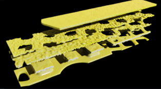
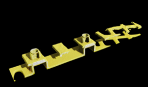
High resolution non-destructive nano-CT of 3D package
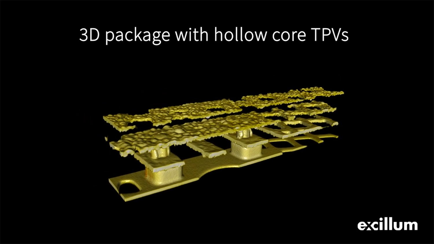
Investigation of a 3D package with hollow core through package vias (TPV) and 3D redistribution layers (RDL). The metal thickness is around 7 µm and roughness can clearly be seen. In addition, improper metalization etc can be detected. A virtual cross section from the 3D X-ray measurement is compared to a SEM cross section.
3D render.
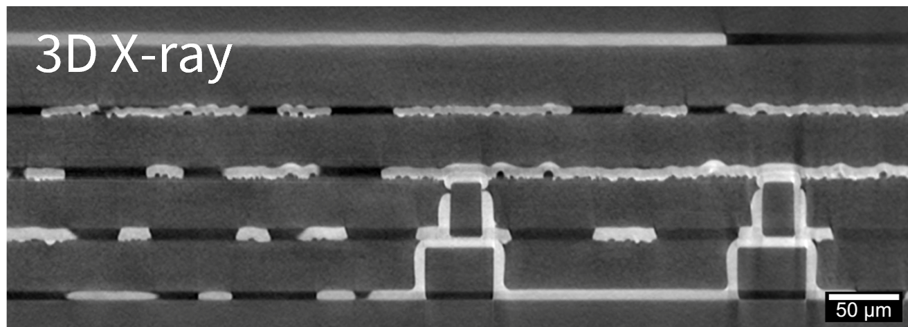
Virtual cross section.
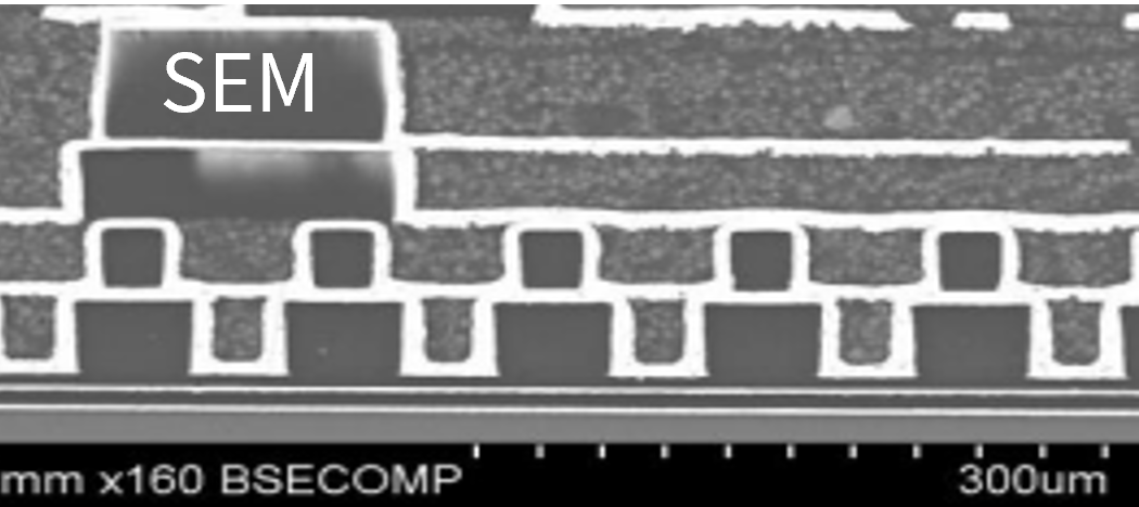
Thanks to Ayad Ghannam at 3DiS for providing the sample.
Want a demonstration?
Are you a manufacturer and want to know how to push beyond the limits of even today’s most state-of-the art X-ray techniques? Book a demo with us!
Book a demo
Powered by partnerships
Excillum’s sources are an integral part of system development for some of the most trusted names in X-ray instrumentation. Together, we work intensely to put the benefits of MetalJet and NanoTube sources into the hands of users everywhere.