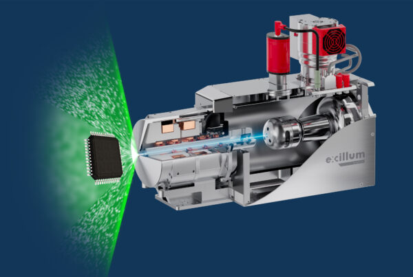
Complex architectures with intricate interconnects, stacked dies, and buried features – the recent developments in advanced packaging come with great possibilities but also challenges. From off-line Failure Analysis (FA) to at- and in-line inspection in manufacturing — more efficient and higher resolution methods are needed to accelerate development and improve yield. X-ray nano-computed tomography (nano-CT) addresses this challenge by offering 3D imaging for e.g. Failure Analysis with sub-micron resolution, enabling precise visualization of internal structures such as micro-bumps, TSVs, bond lines, and voids.
Related Posts
 Publications
Decision-quality fast CT for battery inspection
Steffen Masuch and Klaus Dröder, TU Braunschweig; and Sophie Gräfnitz, PowerCo.
Ingrid AksnesMarch 26, 2026
 Publications
Extremely high-speed X-ray radiography at micrometer resolution to reveal hidden dynamics for failure and root cause analysis of electronics
Julius Hållstedt, Emil Espes, Till Dreier, and Daniel Nilsson, Excillum; Spyridon Gkoumas, DECTRIS Ltd.
Ingrid AksnesDecember 2, 2025
 Publications
Laminography: A non-destructive 3D X-ray breakthrough for advanced packaging
Till Dreier and Julius Hållstedt, Excillum.
Ingrid AksnesOctober 8, 2025
