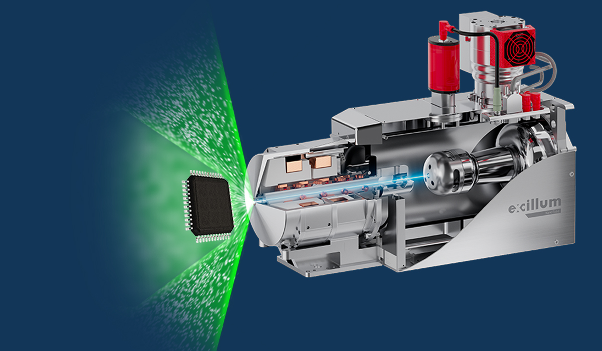
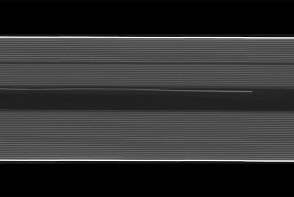
This article highlights X-ray laminography as a powerful alternative to conventional CT for non-destructive 3D inspection of flat, large semiconductor samples such as wafers and advanced packages. Unlike CT, which requires full rotation and often destructive sample preparation, laminography uses a tilted planar rotation that keeps the sample close to the source, enabling high magnification, high throughput, and preservation of sample integrity. By designing an imaging system with a state-of-the-art nanofocus X-ray source allowing for sufficient magnification while assuring a stable system and reliable sample rotation, sub-micron laminography is achievable.