From synchrotron to home laboratory with a 9 keV high intensity HAXPES-Lab
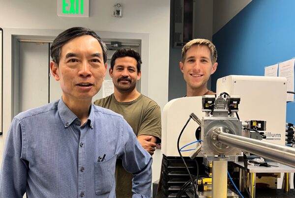
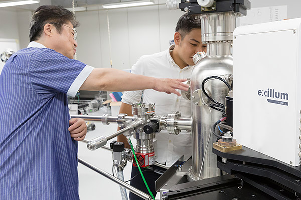
In the laboratory, led by Professor Atsushi Ogura, the objective is to improve the performance of solar cells and electronics devices based on semiconductor nanotechnology. In October 2018, a significant improvement in material characterization capability was achieved when the Scienta Omicron HAXPES-Lab system was installed. The HAXPES-Lab is a home laboratory-type hard X-ray photoelectron spectroscopy (HAXPES) system with the key components: monochromator, high energy analyzer and a 9 keV X-ray source, the Excillum MetalJet D2+.
The non-destructive technique of HAXPES opens up a window to the bulk, as the technique can characterize the element-specific chemical states sub surface of materials, e.g. at buried interfaces or in the bulk. Previously, 9 keV photoemission had only been possible at synchrotron beamlines but with the introduction of the HAXPES-Lab system experiments in the home laboratory became possible.
Lead Researcher
Professor Atsushi Ogura
Institute
Meiji University, School of Science and Technology, Department of Electronics and Biomaterials, Semiconductor Nanotechnologies, Japan
Method
Hard X-ray Photoelectron Spectroscopy (HAXPES)
X-ray sources
Excillum MetalJet D2+
By introducing home-lab HAXPES, continuous measurements for 24 hours a day, 365 days a year became possible. Previously, we were always limited by the available beam time and suffered from long waiting times. But with the HAXPES-Lab we could measure many samples with much faster turnaround from sample preparation, measurement and analysis to refined experiments. This allowed us to significantly accelerate our research and the result was a remarkable improvement in scientific output.

Professor Atsushi Ogura
From synchrotron radiation facility to laboratory
The use of buried interfaces instead of surface layers could be a solution for improving the stability, quality and e.g. to push the performance of materials, such as electronic devices. The drawback is that the layer stack becomes more complex, and the interfaces between the layers become very important. For this reason, methods like Transmission Electron Microscopy (TEM) and X-ray diffraction (XRD) are used to evaluate the physical structure of the interface between different materials. However, the interface chemistry affects the device performance and needs to be evaluated as well.
X-ray photoelectron spectroscopy (XPS) is a most popular method for assessing the chemistry of a sample. However, evaluation of interfaces using XPS is difficult since the energy of photons in traditional XPS is not high enough for photoelectrons from buried interfaces to be detected as they are scattered within the material. By applying X-ray photons with higher energy, Hard energy XPS (HAXPES) this problem can be solved. Having a home-lab HAXPES system with a traditional X-ray source can be both impractical and difficult since the probability of photoelectron generation decreases with the increase in X-ray energy. Only X-ray sources with enough monochromatized flux can be used and HAXPES has therefore mainly been performed at synchrotron facilities. However, the number of utilizable HAXPES synchrotron beamlines is very limited, and the number of research groups in need of HAXPES is great, thereby reducing the access for researchers to short time slots.
X-ray photoelectron spectroscopy (XPS) is a most popular method for assessing the chemistry of a sample. However, evaluation of interfaces using XPS is difficult since the energy of photons in traditional XPS is not high enough for photoelectrons from buried interfaces to be detected as they are scattered within the material. By applying X-ray photons with higher energy, Hard energy XPS (HAXPES) this problem can be solved. Having a home-lab HAXPES system with a traditional X-ray source can be both impractical and difficult since the probability of photoelectron generation decreases with the increase in X-ray energy. Only X-ray sources with enough monochromatized flux can be used and HAXPES has therefore mainly been performed at synchrotron facilities. However, the number of utilizable HAXPES synchrotron beamlines is very limited, and the number of research groups in need of HAXPES is great, thereby reducing the access for researchers to short time slots.
The HAXPES-Lab provides a compact and high-performance home-lab equipment enabling 24/7 access with results far beyond our expectations.
Photoelectron spectroscopy with hard X-ray source realized in laboratory
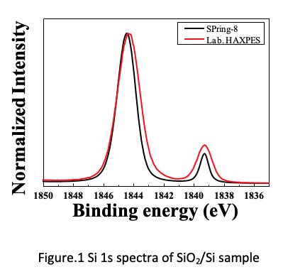
To illustrate the performance and capability of HAXPES-Lab, Figure 1 shows the comparison of SPring-8 and home-lab measurement of a SiO2/Si structure. The sample has a 30-nm-thick SiO2 film grown on a Si substrate by thermal oxidation. The peaks in the vicinity of 1839 eV and 1843 eV are attributed to Si-Si and Si-O bonds, respectively. Both measurements in Figure 1 shows a clear signal originating from the Si-Si chemical state even though it is buried under 30 nm of SiO2. Using a standard XPS tool with an Al or Mg source it would have been virtually impossible to detect this Si-Si feature. In addition, it is noted that the results from SPring-8 and HAXPES-Lab are almost identical.
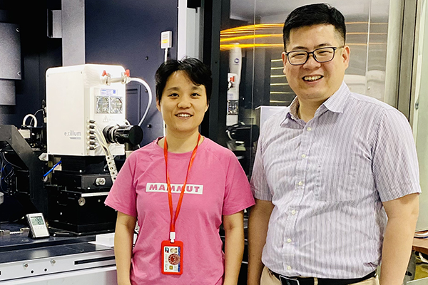
Since the start-up of the HAXPES-Lab at Meiji University, many people have shown interest, and the university has received requests for demonstrating the equipment and to conduct
measurements.
Since the installation of the equipment in October 2018, experiments have been conducted continuously. HAXPES is expected to be very useful for a broad range of applications outside electronic devices, such as biomaterials and similar fields. But due to the limited access to synchrotron HAXPES, many scientists are still unfamiliar with the technique. Therefore, the group led by Professor Ogura believe that one of their most important tasks is to continue to explore the possibilities of home-lab HAXPES and communicate the findings to a broader scientific community.
About HAXPES-Lab
HAXPES-Lab is a laboratory system hard X-ray photoelectron spectrometer designed and manufactured by Scienta Omicron, with the Excillum MetalJet D2+ X-ray source at the core.
HAXPES-Lab explained
Dr. Marcus Lundwall and Dr. Susanna Eriksson from the Electron Spectroscopy team at our partner Scienta Omicron share the features and capabilities of the HAXPES-Lab.